Digital Electronics Part II : Sequential Logic
These pages are © 2011-2015 Kael HANSON
Introduction
You learned in the first section on combinational logic
how to form logic circuits whose outputs depended only on the state of the inputs.
Now, we consider circuits that remember the history of the inputs.
The SR Flip-Flop
The basic sequential circuit element is the SR flip-flop (or bistable multivibrator,
if you prefer the technical term). It can be formed from two NAND gates:
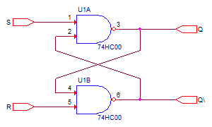
|
| Figure 1: SR Flip-flop from NAND gates |
The function can be understood by including the state of the outputs along with
the inputs, realizing that there are propagation delays inside the gates (of order
5-10 ns for the HC logic that we will use in the labs) that prevents the output
from appearing immediately after the input:
| STATE | S | R | Qn | Q'n |
Qn+1 | Q'n+1 |
|---|
| S0 | 0 | 0 | 0 | 0 | 1 | 1 |
| S1 | 0 | 0 | 0 | 1 | 1 | 1 |
| S2 | 0 | 0 | 1 | 0 | 1 | 1 |
| S3 | 0 | 0 | 1 | 1 | 1 | 1 |
| S4 | 0 | 1 | 0 | 0 | 1 | 1 |
| S5 | 0 | 1 | 0 | 1 | 1 | 1 |
| S6 | 0 | 1 | 1 | 0 | 1 | 0 |
| S7 | 0 | 1 | 1 | 1 | 1 | 0 |
| S8 | 1 | 0 | 0 | 0 | 0 | 1 |
| S9 | 1 | 0 | 0 | 1 | 0 | 1 |
| SA | 1 | 0 | 1 | 0 | 1 | 1 |
| SB | 1 | 0 | 1 | 1 | 0 | 1 |
| SC | 1 | 1 | 0 | 0 | 1 | 1 |
| SD | 1 | 1 | 0 | 1 | 0 | 1 |
| SE | 1 | 1 | 1 | 0 | 1 | 0 |
| SF | 1 | 1 | 1 | 1 | 0 | 0 |
The states have been labeled 0-F: note that the following state transitions occur:
- S0,1,2,3 → S3
- S4,5 → S7 → S6
- S8 → S9
- SA → SB → S9
- SC ↔ SF
- SD → SD
- SE → SE
Therefore, if the oscillatory states SC and SF are avoided, the SR
flip-flop will end up in one of the terminal states S3,
S6, S9, SD, SE. Another more practical
way of looking at the SR behavior is to summarize its function in the abbreviated
table:
| S | R | Q | Q' |
|---|
| 1 | 1 | no change |
| 0 | 1 | 1 | 0 |
| 1 | 0 | 0 | 1 |
| 0 | 0 | forbidden |
As long as both inputs S (commonly called the SET input) and R (commonly called
the RESET input) are high and the flip-flop outputs are complemented (that is,
either 0, 1, or 1, 0), the flip-flop remembers the state. Any time the
circuit must be brought into a known state, either toggle S to set the Q output
high (and thus Q' low) or toggle R to reset Q and set Q'. While this might seem
like a very convenient memory structure, in fact there are better, more useful
ones. Nevertheless, the SR flip-flop plays an important rôle in several later
sequential circuits that we shall come to imminently.
Note that the SR can alternately be implemented using NOR gates. In this case the
sense of S and R is inverted. See the circuit and associated truth table in the
following.
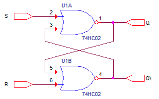
|
| S | R | Q | Q' |
|---|
| 0 | 0 | no change |
| 1 | 0 | 1 | 0 |
| 0 | 1 | 0 | 1 |
| 0 | 1 | forbidden |
|
| Figure 2: SR Flip-flop from NOR gates |
Edge-triggered Logic: Flip-Flops
If you spend any time doing digital design on circuits that are non-trivial
you will eventually come face-to-face with digital logic pathologies that haunt
your circuits and make your life generally less pleasant. By far the most common
problems with modern circuits involve race conditions where pulses are not reaching
their desitination in time, coming either too late or perhaps even too early. This leads to
runt pulses and setup time violations which can cause erratic behaviors
which is difficult to debug. Even though digital pulses are quantized in voltage, the
time behaviors of gates is still a continuous parameter which is unfortunately device,
temperature, and even instance dependent. In order to defensively design the circuit to
be robust against these subtle timing errors, you must resort to worst-case design
where the limiting cases must be verified to still produce correct
operation of the circuit.
The complexity of large designs with hundreds or thousands of signals can be
effectively managed using a technique called synchronous design where
signals are partitioned into or more more clock domains and signal
transitions are driven off of the clock edges. For this reason, sequential
circuit elements which respond to their inputs and change their outputs at,
or at least close by in time to, transitions of other input signals turn out
to be extremely useful.
Master-Slave Flip-Flops
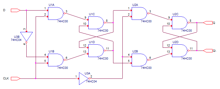
|
| Figure 3: Master-slave flip-flop triggered on the negative edge
of the CLK |
The Master-Slave flip-flop should perhaps be named a dual-stage flip flop. Its operation
can be simply understood by diving the circuit into two pieces each of which is active of
alternate phases of the CLK. When the CLK is high the NAND gates U2A and U2B see the
inverted low signal - thus their output is held at 1 and the slave SR formed by U2C and
U2D maintain the output state. Meanwhile, if D is 0 the input to the master SR U1C, U1D
will be 1 0, forcing a reset of it's output, and if D is 1 the master SR is set. Now,
that the CLK falls to low state. Now the master SR holds its output constant because the
low CLK pulls the outputs of U1A and U1B hight, while the slave SR can now read the
state that was transferred into the master SR output during the previous CLK high period.
In fact, whatever the state was just before the CLK falling edge transition. The output
changes only in response to the falling edge and is decoupled from the input for all times
except the period immediately before the falling CLK edge.
D Flip-Flops
The internal circuit of a D flip flop (or simply DFF) is shown below. For the sake of
explanation, let's call the outputs of the left-most column of NAND gates X, R, S, and Y
from bottom to top (X = output of U1D, R = output of triple-NAND U3A, S = output of U1B,
and Y = output out U1A). When CLK is low U3A and the U1B will pull their outputs high
regardless of the other inputs. Thus, R = H and S = H. This forces the output SR flip
flop to maintain its state. However, the state of D is still "loaded" into the front
of the DFF: Y = D and X = D'. When the CLK suddenly goes high X = D', R = D, S = D',
and Y = D where D is as it was before the transition. This produces
the state D and D' at the outputs Q and Q', respectively.
Now consider the case where D changes while the CLK is held high. In this case
X = H because (DD')' = H, Y = D, S = D', and R = D. Note that S and R are unchanged.
Therefore the outputs will not change again until the next rising edge of CLK.
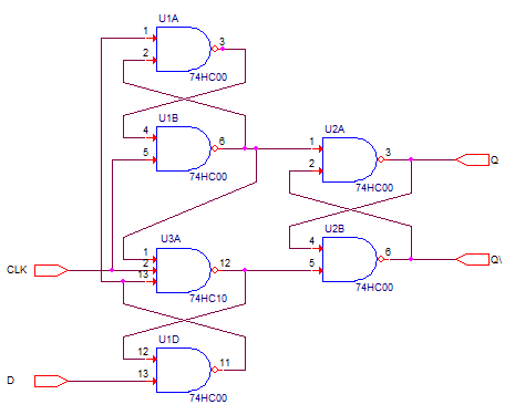
|
| Figure 4: Positive-edge triggered D flip-flop |
The ouputs of these flip-flops simply track the D inputs. However, the
important point is that the ouput only changes following a transition (an edge
is what it is usually called) on the CLK: positive for the D flip-flop above and
negative for the M-S flip flop, however, variants of both types are available
which trigger on the other edges as well.
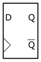
The logic symbol and function table for the positive-edge-sensitive logic is
given:
where the ↑ means action on the positive edge. For the
Master-Slave FF the ↑ would be
replaced by ↓ to signify action on the negative going edge.
These D flip-flops are used throughout digital designs to synchronize
logic signals by aligning them with clocks and to store states
in finite state machine designs as we will see shortly. In addition
the basic logic cells of FPGAs and CPLDs contain one or more flip-flops
- also known as registers especially in the context of these programmable
logic devices.
The DFF function table is also written as
which unfortunately does not specify the clock edge which the device responds to.
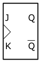
JK Flip Flops
JK flip flops are slightly more versatile variants of the D flip flop, however
not as popular because really most of what one wants to do with flip flops
can already be accomplished with the D. Nevertheless, to be complete and so
that you know they are there and what they do ... here is the function table
and the circuit symbol:
| J | K | Qn+1 |
|---|
| 0 | 0 | Qn |
| 0 | 1 | 0 |
| 1 | 0 | 1 |
| 1 | 1 |
Qn |
|
|
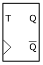
T Flip Flops
Some programmable logic devices contain T ("toggle") flip flops:
Simple Constructions with Flip Flops
Before getting into the gory details of some larger constructions in digital
circuitry, let's look at a few intermediate circuit blocks that are built from
flip flops.
Ripple Counters
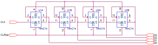
|
| Figure 5: Binary ripple counter from DFFs. |
By connecting the DFF negated ouputs to the D input and chaining the Q output
of one DFF to another as seen in the diagram above, it is possible to make a
simple binary counter. This is called a ripple counter as the clock ripples
through the array of flip flops. A simulation of the ouput of such a counter
is shown in the figures below. Note that the clock frequency is halved at each
DFF output; for this reason the configuration is sometimes called a divide by
16 (or in general divide-by-2N where N is the number of DFFs).
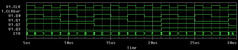 |
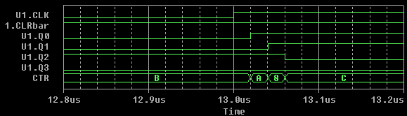 |
| Figure 6: Simulation of the ripple counter. The bottom
plot illustrates one of the problems with the ripple counter: the outputs
cycle through multiple states at the clock edges before finally settling on
the stable output. |
Shift Registers
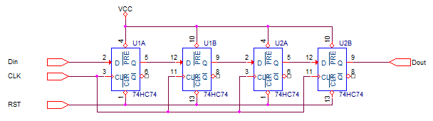
Another example of a useful circuit, actually a finite state machine in its own
right, is the shift register of Figure 7. At each clock pulse, the output propagates
through the flip-flops from left-to-right to appear eventually at the output delayed
by 4 clock cycles and synchronized to the edges of CLK. A simulation is shown below.
This construction is useful itself in state machines to implement "1-hot" state
variables in FPGA where register resources are plentiful. More on this in a bit.
|
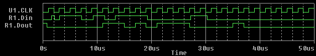 |
| Figure 7: Shift register circuit implementation and simulation. |
Memories
TBD
Clocks and One-Shots
Monostables
The monostable or 'one shot' will output pulses of programmable (via selection of RC
external components) width triggered by an edge on one of the input signals. These
devices are handy for trigger circuits: gate widths and delays can be setup easily.
See the data sheet
of the popular '123 a dual one-shot with flexible inputs.
However, the timing components are analog in nature so one must deal with variations
due to temperature, time, manufacturing, ... A more robust technique uses 100% digital
state machines and well-controlled clocks.
'555 Timer Chip
The '555 was a popular clocking chip able to achieve modest speeds of up to 1 MHz.
See the ICM7555 data
sheet for an explanation of the chip along with some popular applications: astable
(clock), monostable, ...
Finite State Machines
This is such a large topic that it gets to live in
its own webpage.