Digital Electronics Part I : Combinational Circuits
These pages are © 2011-2015 Kael HANSON
Introduction
So that it may serve to later clarify the important design concepts of
synchronous versus asynchronous circuit design, I follow the classical approach
and introduce two broad sub-divisions of digital circuits:
- Combinational
- Circuits whose output depends only on the current state of the
inputs.
- Sequential
- Circuits whose output depends on the history as well as the current
state of the inputs.
We shall begin with the simpler combinational configurations before advancing to
sequential circuits. In general, one would have to look hard to find a complete
circuit with only combinational elements, however, in pratice, large and complex
sub-units of a complete design hierarchy can be entirely combinational in nature
and moreover, as will be shown later, sequential circuits are themselves composed
of logic gates with feedback.
So, let's begin with an example of a circuit which might be of interest to an
experimental physicist.
Example Implementation: Muon Cosmic Ray Experiment Trigger
|
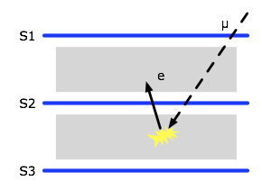
| Figure 1: Muon decay cosmic ray experiment |
The first is a very specific example of a cosmic ray experiment where one wants to
capture cosmic ray muon decay events. The apparatus consists of 3 planes of scintillator
and two boxes of high density material: sand or rock or something even heavier. Muons
are very penetrating particles which will pass the absorber easily and ionize the
scintillators producing light which is picked up by photomultipliers (PMTs) coupled to
each scintillator plane. The photomultipliers produce large electrical pulses (10's to
100's of mV) which can be fed through a discriminator to produce logic level pulses.
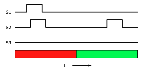
Now, consider the case of a cosmic ray (CR) muon entering the apparatus as shown in
Figure 1. A possible schematic of the electronic signals this experiment might
produce are shown in Figure 2. Scintillator plane S1 is hit first and then S2
slightly later due to time-of-flight of the muon (3 ns per meter traveled). The hits
somehow produce the logic signals shown. Were the muon to continue instead
of decaying between planes 2 and 3, one would also observe a 3rd hit in S3. However,
in this example the muon comes to rest between planes S2 and S3, decays some 100's
of nanoseconds or µs later, and emits an electron which travels back through
plane S2 and produces a second pulse in S2. The electron could also travel downward
and strike plane S3 at a later time and be distinguishable from a non-decaying muon.
In order to capture events of this nature one would like to design a circuit that
triggers when:
- There is a coincidence of hits within a small time window, several ns
depending on the spacing, in planes S1 and S2,
- There is no signal in plane S3 coincident with S1 and S2,
- There is a late hit in either S2 or S3.
The decay is a random process with a mean of 2.2 µs, therefore there is
an entire range of possible times following the signals in S1 and S2
which should be accepted (the green bar region in the Figure, for example).
 |
| Figure 2: Digital signals produced in the muon decay experiment |
The 3rd condition will be the subject of a later discussion when we arrive at
sequential logic. The first two conditions state that we want signals in
S1 and S2 and not S3. This is typically written as a logic
expression
Logic Signals
It is evident that the signals being processed by this example trigger system
are not the raw PMT signals which would have a complex form dependent on
the amount of energy deposition in the scintillator, rather they are
square pulses of fixed width and fixed height that only serve to
mark the presence (or absence) of a hit in the photomultiplier. This ideal can be
realized by using a pulse discriminator which emits pulses of constant height and
a monostable to set the width in time. Because there are in principle only two
possible voltage levels, the signals can be treated as being in one of two logic
states: logic HIGH and logic LOW. By interpreting these states as TRUE and FALSE
we can use logic gates to act on the digital input signals S1,
S2, and S3, and produce a digital output which corresponds
to the logic expression (1).
Logic Gates
These logic gates are available as integrated circuit packages, often with multiple
gates per package and with a. A popular, industry-wide standard set of
IC's known as the 7400-series logic dates back to the 1960's and still
is actively being produced by many manufacturers. The following table lists some
of the basic logical expressions, their truth tables, circuit
symbols, and the corresponding 7400-series ICs:
| Gate Name | Expression | Standard Symbol | IEC Symbol |
Truth Table | 7400-series IC |
|---|
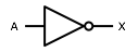
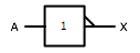
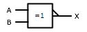
| NOT |
X = A
X = A' |
 |
 |
|
|
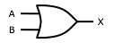
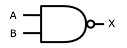
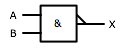
| AND |
X = A · B
X = AB |
 |
 |
|
| 7408 | Quad 2-input |
| 7411 | Triple 3-input |
| 7421 | Dual 4-input |
|
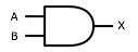
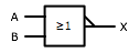
| OR |
X = A + B |
 |
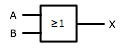 |
|
|
| XOR |
X = A ⊕ B |
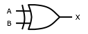 |
 |
|
|
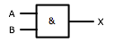
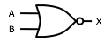
| NAND |
X = A · B |
 |
 |
|
| 7400 | Quad 2-input |
| 7401 | Quad 2-input, open collector outputs |
| 7410 | Triple 3-input |
| 7420 | Dual 4-input |
| 7430 | Single 8-input |
|
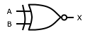
| NOR |
X = A + B |
 |
 |
|
| 7402 | Quad 2-input |
| 7427 | Triple 3-input |
| 7425 | Dual 4-input |
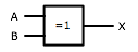
|
| XNOR |
X = A ⊕ B |
 |
 |
|
|
Logic Identities
Boolean logic identities are summarized below:
- 1' = 0
- A · A = A
- A + A = A
- A · 1 = A
- A + 1 = 1
- A · 0 = 0
- A + 0 = A
- A · A' = 0
- A + A' = 1
- (A · A)' = A'
- (A + A)' = A'
- A · (B + C) = A · B + A · C
- (A + B) · (A + C) = A + B · C
- (A)' = A
- A + A'B = A + B
- AB = BA
- A + B = B + A
- A(BC) = (AB)C
- A ⊕ B = A'B + B'A
And finally there are the laws of DeMorgan which can switch AND / OR operations:
- (AB)' = A' + B'
- (A + B)' = A'B'
DeMorgan's laws have the consequence that all combinational logic circuits could be
constructed out of NAND or NOR gates (but not AND or OR gates). Take as
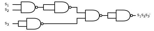
example the muon trigger system; one may desire to construct the logic completely from
7400 NAND gates since there are 4 to a package. The logic expression could be re-written
as the following sequence of logical identities:
Y = (S1S2)'
X = ((YY)'(S3S3)')'
|
(2) |
This requires 5 NAND gates to implement which would appear as the circuit:
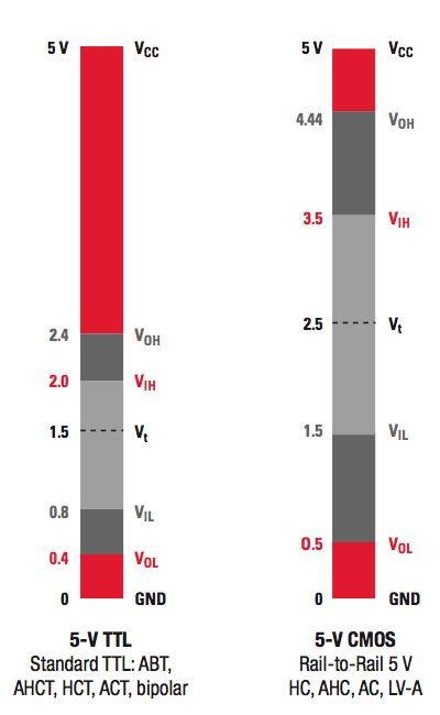
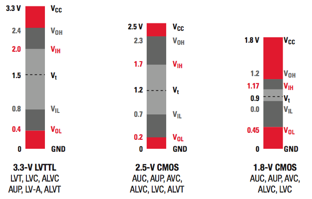
Logic families and logic thresholds
Each logic family defines thresholds for valid high and low
levels:
- VIL
- The voltage region in which the logic gate considers the
input to be LOW or logic FALSE.
- VIH
- The voltage region in which the logic gate considers the
input to be HIGH or logic TRUE.
- VOL
- The maximum voltage at the output for a logic LOW output.
- VOH
- The minimum voltage at the output for a logic HIGH output.
Table: Logic thresholds for various logic families.
| Family | VCC |
VIL | VIH |
VOL | VOH |
Comments |
| Min | Max | Min | Max |
Min | Max |
| TTL | 4.75 | 5.25 |
- | 0.8 | 2 | - |
0.4 | 2.4 |
| LVTTL | 2 | 5.5 |
- | 0.3×VCC |
0.7×VCC | - |
0.4 | 2 |
At VCC = 2.3 V to 2.7 V |
| - | 0.3×VCC |
0.7×VCC | - |
0.44 | 2 |
At VCC = 3 V to 3.6 V |
| - | 0.3×VCC |
0.7×VCC | - |
0.55 | 2 |
At VCC = 4.5 V to 5.5 V |
| HCMOS | 2 | 6 |
GND | 0.5 |
1.5 | VCC |
0.1 | 1.9 |
At VCC = 2 V |
| GND | 1.35 |
3.15 | VCC |
0.1 | 4.4 |
At VCC = 4.5 V |
| GND | 1.8 |
4.2 | VCC |
0.1 | 5.9 |
At VCC = 6 V |
| LVCMOS | 2 | 3.6 |
GND | 0.7 |
1.7 | VCC |
0.4 | 2.2 |
At VCC = 2.7 V |
| GND | 0.8 |
2 | VCC |
0.55 | 2.4 |
At VCC = 3 V |
This is illustrated in the following graphs which were taken from the
Texas Instruments™ Logic Guide.
Inverters and Boolean Gates : Transistor Implementation
Demonstration with an ideal switch
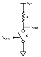 |
| Figure 3: Simple switch inverter |
Transistors switches internally compose the circuits of the logic gates discussed
previously. Let's consider the trivial example of the circuit shown at right to
understand the basic principle behind an inverter. The switch will be in the open
state (non-conducting) if VCTRL is below some threshold voltage, VT,
nominally VCC/2, and will be closed (conducting) if it is above VT.
- If VCTRL is in a HIGH state then the switch is closed. The output
is grounded (VOUT in LOW logic state).
- If VCTRL is in a LOW state the switch is open. The output is pulled
up through the output resistance R.
Therefore, the output follows the logic inverse of the input: a NOT gate.
Transistor inverter
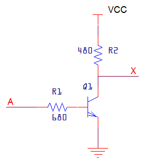
|
| Figure 4: BJT inverter |
A BJT inverter is shown in the graphic at left. It works as follows: assuming
a VCC of 5 V, then if point A is above about 0.8 V, the transistor
will enter saturation as the collector current increases to the point where
the voltage drop across resistor R2 is too great to keep the base-collector
junction reverse-biased. Q1 will pull the collector, and thus the output, X,
to approximately 0.05 V. Conversely, if point A is below about 0.6 V the transistor
is cut-off, no current flows, and point X is pulled up through 480 Ω to
logic HIGH.
Were the BJT replaced by a MOSFET, one could get rid of the base resistor as the
FET gate draws no current. The
MOSFET drain-source channel will act as a low-impedance (a few ohms are typical)
path if VGS, the potential difference between the gate and the source
is above VT which is typically in the range of several volts, it is a
characteristic of each MOSFET.
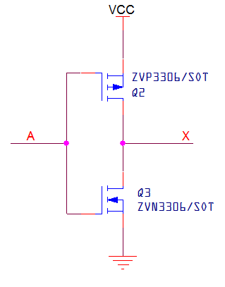
|
| Figure 5: CMOS inverter
|
CMOS Inverter
The problem with such inverter circuits is that, as you may have noticed, for
outputs at logic LOW, quite a bit of power can be dissipated through the pull-up
resistor. The resistor can be made arbitrarily large but with a penalty in
switching speed. A better solution is to have a pair of transistors of which
only one is conducting at any time far enough away from an output state
transition. This is shown in Figure 5. The CMOS (Complementary MOS) basic
structure shown here forms the foundation of much of modern digital circuits.
It is made from a p-channel MOSFET (Q2) and an
n-channel MOSFET (Q3). When A is HIGH Q2 is OFF and Q3 is ON, thus X
is LOW. When A is LOW, Q2 is ON and Q3 is OFF, thus X is HI. Note that
in each case only 1 output transistor is ON at any point, thus there is
no quiescent power dissipation.
CMOS NAND gate
TBD
Open Collector and Three-State Outputs
TBD
Numeric Computing
Binary Numbers: Introduction to Number Bases
A single output of a digital gate can be in one of two states: 0 or 1. A pair of
independent ouputs can be in one of four states: (0, 0), (0, 1), (1, 0), (1, 1).
In general, the outputs of N gates, Q0, Q1, ..., QN,
can hold 2N states. These states may represent numbers, a representation
which has powerful consequences when circuit elements which perform numerical
operations such as addition and subtraction are introduced. This will be done
shortly. For the present, we occupy ourselves with understanding the representation
of numbers using sequences of HIGH/LOW logic states: this is the system of binary numbers.
Table C: Enumeration of 4-bit binary (base 2) numbers in decimal (base 10),
octal (base 8), and hexadecimal (base 16).
| Q3Q2Q1Q0 |
Decimal | Octal | Hexadecimal |
| 0000 | 0 | 0 | 0 |
| 0001 | 1 | 1 | 1 |
| 0010 | 2 | 2 | 2 |
| 0011 | 3 | 3 | 3 |
| 0100 | 4 | 4 | 4 |
| 0101 | 5 | 5 | 5 |
| 0110 | 6 | 6 | 6 |
| 0111 | 7 | 7 | 7 |
| 1000 | 8 | 10 | 8 |
| 1001 | 9 | 11 | 9 |
| 1010 | 10 | 12 | A |
| 1011 | 11 | 13 | B |
| 1100 | 12 | 14 | C |
| 1101 | 13 | 15 | D |
| 1110 | 14 | 16 | E |
| 1111 | 15 | 17 | F |
Binary numbers are written as strings of '0' or '1' bits, usually written
most significant bit (MSB) first and
least significant bit (LSB) last, in analogy with decimal numbers. The
corresponding decimal number may be computed using a simple algorithm:
- Starting with the LSB, set b = 0
- Accumulate (add) 2b if the bit is '1'
- Move to the next bit, b = b + 1
Transformation from decimal into binary may be accomplished with the following
algorithm:
- Divide the number by 2 and place the remainder (0 or 1) in LSB
- Repeat this step, appending the bits in the next-most-significant-bit
position (forming the binary string from right-to-left) until the
quotient is zero.
Hexadecimal numbers offer a compact format for
expressing long bit strings. Because the number base is 16, each quartet
of bits orthogonally separates into a hex digit so that the transformation
between binary and hex representations is trivial: for example the rather
long binary string 10 111 010 001 011 110 010 011 111 can be written as
2E8BC9F by consulting Table C. Octal numbers offer an another orthogonal
number format, base 8, with triplets of bits mapping onto a single octal
digit. Thus, the binary string above in octal would be 272136237.
When it is not clear which number base a sequence of digits is expressed in
different conventions are used. Sometimes a number will be tagged with
'bin', 'dec', or 'hex' to resolve the ambiguity:
10010110bin = 226oct = 150dec = 96hex
In the C programming language, and also languages with similar syntax
(C++, Java, Python to name a few), octal literals (constants in the code) may be
denoted as such by a leading '0' which is redundant in decimal. Hexadecimal
literals are expressed with a leading '0x', thus the following C function would
return 1:
int test() {
    int a = 150;
    int b = 0226;
    int c = 0x96;
    return (a == b && b == c);
}
Addition of binary numbers
Despite it being rather more tedious to add binary numbers, there is nothing
difficult at all about the mechanics behind addition in base 2. It is
completely analogous to addition of decimal numbers so let's jump right in
with an example, say the addition using 4-bit adders of 11 + 7:
| 1 | 1 | 1 | 1 | | Cy |
| 1 | 0 | 1 | 1 | A |
| + | 0 | 1 | 1 | 1 | B |
| 1 | 0 | 0 | 1 | 0 |
The process starts with the bits in the right hand column: 1 + 1 = 2 but in binary
that must then be 0 with a carry into the next column as signified by the 'Cy' row
on top. In the next row the three 1's add to 1 with a carry, and so on ...
Finally there is a carry out of the last bit. The resulting number is 18 which
agrees well with the decimal version of this operation. Note that it is often
the case in binary additions that registers are of fixed width and thus there is
no obvious place to put the carry bit in the result. Rather, it would be
truncated to 4-bits giving the odd answer of 0010 = 2 instead of 18.
Table D: Truth table for binary full-adder
| Cin | A | B | X | Cout |
|---|
| 0 | 0 | 0 | 0 | 0 |
| 0 | 0 | 1 | 1 | 0 |
| 0 | 1 | 0 | 1 | 0 |
| 0 | 1 | 1 | 0 | 1 |
| 1 | 0 | 0 | 1 | 0 |
| 1 | 0 | 1 | 0 | 1 |
| 1 | 1 | 0 | 0 | 1 |
| 1 | 1 | 1 | 1 | 1 |
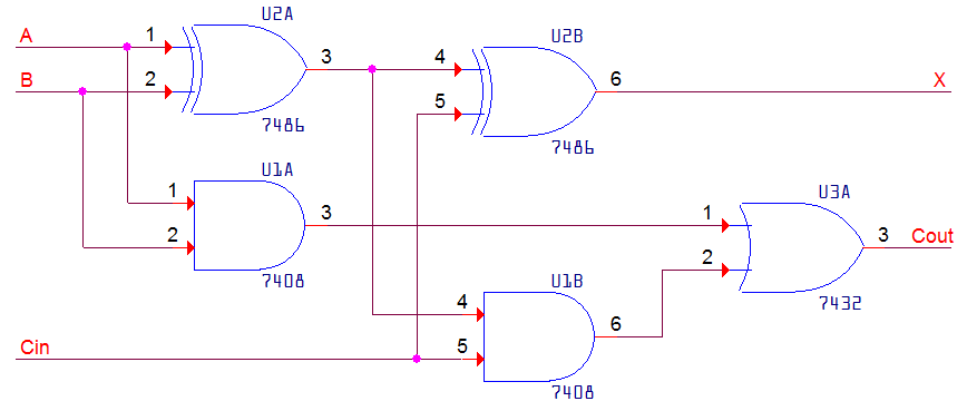
But how is this operation to be undertaken by logic circuits? The solution is
obtained by examination of the truth table that represents the addition of a
single pair of bits - one column in the example. Notice that there are 3
inputs: the bit of A, the bit of B, and the carry bit, and two outputs: the
sum bit and the carry out to the next column bit. We will call the input
carry the carry in or Cin, and the carry out, Cout in the truth
table, Table D.
Notice that the sum output, X, is true when the input lines A, B, and Cin
have an odd number of bits. This may be implemented as the following
logical expression:
X = A ⊕ B ⊕ Cin
while the carry out, Cout, is TRUE when A and B are TRUE or when Cin is TRUE
and A ⊕ B is TRUE:
Cout = AB + (A ⊕ B) · Cin
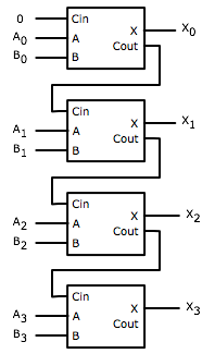
Thus a 1-bit full adder can be realized by the following circuit diagram:
Wider (i.e. more bits) adders are constructed from the single bit basic
building block by chaining the carry out of one stage to the carry in
of the next stage:
Signed and unsigned
The binary representation explained above covers only numbers from 0 to
2N - 1 where N is the number of bits in the binary string. Of course,
it is entirely your business how you enumerate the logic states: the enumeration
listed in Table C is merely one of many possible enumerations and circumstances
particular to an application may favor one of these other possibilities.
Very often, numeric problems involve negative numbers. Numbers that can take on
both negative and positive values are called signed numbers, as opposed to
unsigned numbers which are only positive or zero. An enumeration of states
known as 2's complement allows one to represent signed numbers
and has the important property that the adder developed above for
unsigned numbers all work without modification for signed numbers.
As was seen in the section on addition, adding two N-bit numbers in
general requires N+1 bits to hold the result.
Magnitude Comparators
TBD
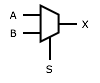
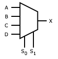
Multiplexers
A multiplexer (also muxer or even mux) takes M signal inputs and N selector
inputs (usually 2N = M) and places the input addressed by
the selector lines onto the output.
| Circuit Symbol | Truth Table | Description |
|---|
 |
|
2-input multiplexer |
 |
| A | B | C | D |
S1 | S0 |
X |
| 0 | X | X | X |
0 | 0 | 0 |
| 1 | X | X | X |
0 | 0 | 1 |
| X | 0 | X | X |
0 | 1 | 0 |
| X | 1 | X | X |
0 | 1 | 1 |
| X | X | 0 | X |
1 | 0 | 0 |
| X | X | 1 | X |
1 | 0 | 1 |
| X | X | X | 1 |
1 | 1 | 0 |
| X | X | X | 1 |
1 | 1 | 1 |
|
4-input multiplexer |
|
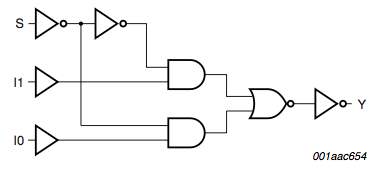
| Figure 8: Internal diagram for the NXP 74LVC1G157. |
Demultiplexers and decoders
The inverse circuit is called a demultiplexer or a decoder.
It takes N selector
inputs, usually called address inputs, and activates one of the
2N outputs. This circuit is often used to activate
circuitry interconnected using a shared data bus. Another
application of decoders is as a driver for a 7-segment display.
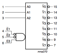
Logic symbol and truth table for '138 3-to-8 line decoder
(from NXP Semiconductor datasheet). Note that the outputs
are ACTIVE LOW.
| E1' | E2' | E3 |
A0 | A1 | A2 |
Y0' | Y1' | Y2' | Y3' |
Y5' | Y5' | Y6' | Y7' |
| 1 | X | X |
X | X | X |
1 | 1 | 1 | 1 |
1 | 1 | 1 | 1 |
| X | 1 | X |
X | X | X |
1 | 1 | 1 | 1 |
1 | 1 | 1 | 1 |
| X | X | 0 |
X | X | X |
1 | 1 | 1 | 1 |
1 | 1 | 1 | 1 |
| 0 | 0 | 1 |
0 | 0 | 0 |
0 | 1 | 1 | 1 |
1 | 1 | 1 | 1 |
| 0 | 0 | 1 |
0 | 0 | 1 |
1 | 0 | 1 | 1 |
1 | 1 | 1 | 1 |
| 0 | 0 | 1 |
0 | 1 | 0 |
1 | 1 | 0 | 1 |
1 | 1 | 1 | 1 |
| 0 | 0 | 1 |
0 | 1 | 1 |
1 | 1 | 1 | 0 |
1 | 1 | 1 | 1 |
| 0 | 0 | 1 |
1 | 0 | 0 |
1 | 1 | 1 | 1 |
0 | 1 | 1 | 1 |
| 0 | 0 | 1 |
1 | 0 | 1 |
1 | 1 | 1 | 1 |
1 | 0 | 1 | 1 |
| 0 | 0 | 1 |
1 | 1 | 0 |
1 | 1 | 1 | 1 |
1 | 1 | 0 | 1 |
| 0 | 0 | 1 |
1 | 1 | 1 |
1 | 1 | 1 | 1 |
1 | 1 | 1 | 0 |
|
|
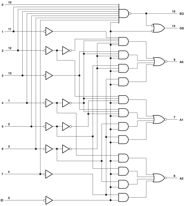
Priority Encoders
A priority encoder takes N inputs and outputs the address of the highest set
bit. The '148 offers this function with ACTIVE LOW inputs and outputs, and
is cascadable using EI' and EO':
| EI' | I0' | I1' | I2' | I3' |
I4' | I5' | I6' | I7' |
A2' | A1' | A0' | GS' | EO' |
| 1 | X | X | X | X |
X | X | X | X |
1 | 1 | 1 | 1 | 1 |
| 0 | 1 | 1 | 1 | 1 |
1 | 1 | 1 | 1 |
1 | 1 | 1 | 0 | 1 |
| X | 0 | 1 | 1 | 1 |
1 | 1 | 1 | 1 |
1 | 1 | 0 | 0 | 1 |
| X | X | 0 | 1 | 1 |
1 | 1 | 1 | 1 |
1 | 0 | 1 | 0 | 1 |
| X | X | X | 0 | 1 |
1 | 1 | 1 | 1 |
1 | 0 | 0 | 0 | 1 |
| X | X | X | X | X |
1 | 1 | 1 | 1 |
0 | 1 | 1 | 0 | 1 |
| X | X | X | X | X |
X | 0 | 1 | 1 |
0 | 1 | 0 | 0 | 1 |
| X | X | X | X | X |
X | X | 0 | 1 |
0 | 0 | 1 | 0 | 1 |
| X | X | X | X | X |
X | X | X | 0 |
0 | 0 | 0 | 0 | 1 |
|
|