Operational Amplifier Noise |
|
This article discusses the noise generated within op amps and their associated circuitry, not external noise which they may pick up. External noise is important, and has been discussed in detail elsewhere, but here we are concerned solely with the internal noise of the op amp and its associated circuitry. There are three noise sources in an op amp: a voltage noise, Vn, which appears differentially across the two inputs and a current noise in both the inverting and non-inverting inputs, In- and In+ respectively. These three noise sources are generally analysed as if they are uncorrelated (independent of each other). For most current feedback op amps, and for voltage feedback op amps with simple bipolar junction transistors (BJTs), and, at low frequencies, field-effect transistors (FETs) as input stages this assumption is correct. Bias-compensated op-amps may have some correlation of the current noise in their inverting and non-inverting inputs, and at high frequencies noise in the tail currents of a long-tailed pair of FETs will couple to both their gates via the gate-channel capacitance giving such amplifiers correlated input noise currents at HF. Since these effects are not usually documented on data sheets, and are rarely large enough to be a problem the remainder of this article assumes that op-amp noise currents are uncorrelated. In addition to these three internal noise sources, it is necessary to consider the noise of the external resistors which are used with the op amp. All resistors have thermal or Johnson1 noise of Uncorrelated noise voltages add in a "root sum of squares" manner; i.e., noise voltages V1, V2 & V3 add to give a result of
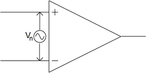
Voltage noise, Vn, appears differentially across op-amp inputs Figure 1 The voltage noise of different op amps may vary from under 1 nV/√Hz to 20 nV/√Hz, or even more. Op amps with BJTs as input devices tend to have lower voltage noise than ones using field-effect transistors, although it is possible to make junction field-effect transistor (JFET) op amps with low voltage noise (such as the AD743/AD745), at the cost of large input devices and hence large (~20 pF) input capacitance. Metal-oxide-silicon field-effect transistors (MOSFETs) tend to be a little noisier than JFETs so CMOS op-amps, though useful for many applications, rarely have very low voltage noise (their current noise is usually excellent). Voltage noise is normally specified on the data sheet, and it is not possible to predict it from other parameters.
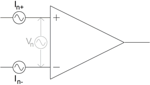
There are (mostly) uncorrelated current noise Figure 2 Current noise can vary much more widely, from around 0.1 fA/√Hz (in JFET electrometer op amps) to several pA/√Hz (in high speed bipolar op amps). It is not always specified on data sheets, but may be calculated in cases (like simple BJT or JFET input devices) where all the bias current flows in the input junction, because in these cases it is simply the shot (or Schottky) noise of the bias current3. The shot noise spectral density is simply
where Ib is the bias current (in amps) and q is the charge on an electron (1.6 × 10⁻¹⁹ C). Op amps that have a more complex input structure, such as bias-compensated types (like the OP07 and all its many descendants), or current feedback op amps, will have current noise that is greater than the shot noise of the bias current since with these devices the bias current is the algebraic sum of several currents flowing in the input nodes and each has, at the very least, its own shot noise. It is not possible to calculate the current noise of these more complex structures from the data normally provided on a data sheet, so unless it is published it is unknown. But it is obvious that the current noise of an op-amp cannot ever be less than the shot noise of its bias current, so if we know the bias current of an op amp we can specify a lower limit to its possible noise current. Voltage feedback op amps have balanced input stages, which means that the inverting and non-inverting inputs have identical structures. This in turn means that the current noise in the inverting and non-inverting inputs are similar in amplitude. This is not the case with current feedback op amps – In- in an AD8003 is 36 pA/√Hz, 12 time larger than its In+ of 3 pA/√Hz, and even the 1/f corner frequencies of the two inputs are different.
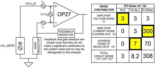
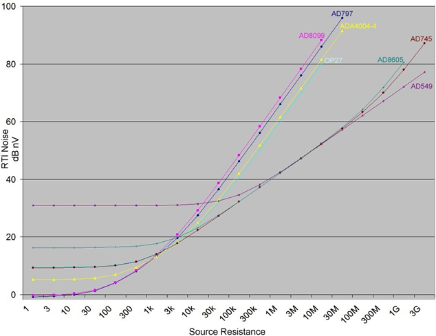
Figure 3 Current noise is only important when it flows in an impedance and generates a noise voltage. The choice of a low noise op amp therefore depends on the impedances around it. In Fig 3 an OP27, a venerable4 but still widely used bias compensated op amp with low voltage noise (3nV/√Hz ) but quite high current noise (1pA/√Hz ), is shown in a non-inverting amplifier. To simplify analysis we shall disregard the effects of the gain resistors and consider the noise contributions referred to the input (RTI) of the amplifier and its source resistance R. With zero source resistance, the voltage noise of 3nV/√Hz will dominate. With a source resistance of 3kΩ, the current noise (1pA/√Hz flowing in 3kΩ) will equal the voltage noise, but the Johnson noise of the 3kΩ resistor is 7nV/√Hz and so here it is dominant. With a source resistance of 300kΩ, the current noise increases a hundredfold to 300nV/√Hz, while the voltage noise continues unchanged, and the Johnson noise (which is proportional to the square root of the resistance) only increases tenfold. Essentially the voltage noise is independent of source resistance, the Johnson noise of the resistance increases at 10 dB/decade resistance increase, and the noise due to current noise flowing in the source resistance increases at 20 dB/decade. This is clearly shown in Fig 4. It is evident that with a low source resistance the AD797 has remarkably low noise, but at around 3kΩ source resistance there is little difference between any of the amplifiers with low voltage noise because the Johnson noise has become dominant. Above this the bipolar amplifiers with high current noise have the worst performance, while the FET amplifiers continue to be dominated by Johnson noise rather than their own current noise until we reach very high values of resistance. We thus see that the choice of a low noise amplifier does not depend simply on its voltage noise, but on its current noise and the source impedance of the system in which it is to be used. Note that if the source impedance is reactive it will not give rise to Johnson noise, but it will still produce a voltage when noise current flows in it. In the case of the AD549, which has quite poor voltage noise of 35 nV/√Hz, the current noise is so low that it only becomes greater than the Johnson noise at source resistances of greater then 1 TΩ (1012 Ω). But the input capacitance of the AD549 is about 1 pF, which shunts the source resistance, so even with the most careful layout it is only possible for the source impedance to exceed 1 TΩ at frequencies below 0.16 Hz, which is far below the AD549's 1/f corner of 100 Hz.
Figure 4 For low impedance circuitry, amplifiers with low voltage noise, such as the AD797, will be the obvious choice, since they are inexpensive, and their comparatively large current noise will not affect the application. At medium resistances, the Johnson noise of resistors is dominant, while at very high resistances, we must choose an op amp with the smallest possible current noise, such as the AD745 or AD549. Until recently FET amplifiers tended to have comparatively high voltage noise (though very low current noise), and were thus more suitable for low noise applications in high rather than low impedance circuitry. The AD8605 and AD743/AD745 have low values of both voltage and current noise. The AD8605 specifications are 7 nV/√Hz and 10 fA/√Hz, and the AD743/AD745 specifications are 2.9nV/√Hz and 6.9fA/√Hz. These make possible the design of low-noise amplifier circuits which have low noise over a wide range of source impedances. So far, we have assumed that noise is white (i.e., its spectral density does not vary with frequency). This is true over most of an op amp's frequency range, but at low frequencies the noise spectral density rises at 3dB/octave as shown in Fig 5. The frequency at which it starts to rise is known as the 1/f corner frequency and is a figure of merit – the lower the better. The 1/f corner frequencies are not necessarily the same for the voltage noise and the current noise of a particular amplifier, and a current feedback op amp may have three 1/f corners: for its voltage noise, its inverting input current noise, and its non inverting input current noise. The assumption that low frequency noise in op amps always rises at 3 dB/octave is another simplification. Inspection of the noise v frequency graphs on many op amp data sheets show that real life™ is not so simple. However it is a valid starting point, and sufficiently accurate for many, if not all, analyses. In addition to 1/f (or whatever!) noise there is another LF noise effect in op-amps – popcorn noise. This consists of random step changes of offset voltage in a timescale of tens of milliseconds or longer, causing the op amp output, if played as audio, to sound like cooking popcorn. In the early days of IC op amps popcorn noise was a very serious problem and one of the most important criteria for op amp selection was low popcorn noise. Although it can still be observed today it is far less of a problem for op amp users since its effects are now well understood and reputable manufacturers can screen devices for popcorn noise during manufacture. That they still sometimes find batches of circuits with poor popcorn noise is evidence that all the mechanisms behind it are still not yet fully understood, but a reassurance to op amp users that such devices are unlikely to pass final test and be sold.
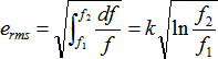
Figure 5 The best bipolar low frequency low noise amplifiers have 1/f corner frequencies in the range 1 20 Hz, while JFET devices and more general purpose op amps have values in the range to 100 Hz5. Very fast amplifiers, however, may make compromises in processing to achieve high speed which result in quite high 1/f corners of several hundred or even thousand Hz. This is generally unimportant in the applications for which they were intended, but will affect their performance at audio frequencies. It is very important to review both the total bandwidth and the low frequency noise requirements of a system before choosing an amplifier. As an example in Fig 4 we see that the AD767 and the AD8099 appear to have very similar noise characteristics – and the AD8099 is less than half the price of the AD797. But looking at other characteristics of these devices we observe that the 1/f corner of the AD797 is at the bottom of the audio spectrum while that of the AD8099 is near the top of it. The AD8099 is much faster than the AD797 but is not as versatile in supply range either. So although its noise is remarkable it is unlikely that we should choose the AD8099 over the AD797 for low noise audio applications. RMS Noise Considerations In the midband (white/constant spectral density) region the total noise is simply equal to the noise spectral density times the square root of the bandwidth. The noise between frequencies f1 and f2, where there is a noise spectral density of Vn nV/√Hz, is
In the 1/f region, the RMS noise in the bandwidth f1 to f2 is given by
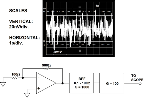
where k is the noise spectral density at 1Hz. The total 1/f noise in a given band is a function of the ratio of the low and high band edge frequencies, since the actual frequency cancels out. It is necessary, however, that the upper band edge is still in the 1/f region for this formula to be accurate. (Note that if the noise/frequency plot on the data sheet shows a wide deviation from the ideal 1/f characteristic a more complex expression than [3] may occasionally be necessary.) In many cases, the low frequency noise is specified as a peak-to-peak value within the bandwidth 0.1 to 10Hz. This is measured by inserting a 0.1 to 10Hz bandpass filter between the op amp and the measuring device. The measurement is often presented as a scope photo with a time scale of 1s/div – the test circuit and a typical display (for the OP213) is shown in Fig 6.
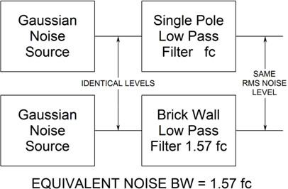
Figure 6 In practice, it is virtually impossible to measure noise within specific frequency limits with no contribution from outside those limits, since practical filters have finite rolloff characteristics. Fortunately, the measurement error introduced by a single pole lowpass filter is readily computed. The noise in the spectrum above the single pole filter cutoff frequency, fc, extends the corner frequency to 1.57fc. Similarly, a two pole filter has an apparent corner frequency of approximately 1.2fc. The error correction factor is small and usually negligible for filters having more than two poles. The bandwidth obtained after applying the correction factor is referred to as the equivalent noise bandwidth of the filter (see Fig 7).
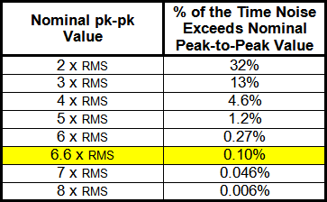
Figure 7 When computing RMS noise for wide bandwidth op amps, 1/f noise becomes relatively insignificant. The dominant source of noise is gaussian, or white noise6. This noise has a relatively constant noise spectral density over a wide range of frequencies. The RMS noise calculation is made by multiplying the noise spectral density by the square root of the equivalent noise bandwidth. Mathematicians tell us that it is impossible to specify a maximum peak-to-peak (pk-pk) noise in a Gaussian system. For a given value of RMS Gaussian noise the chance of a particular peak-to-peak value being exceeded decreases rapidly as that value increases – but the probability never becomes zero. Thus, for a given RMS noise, it is possible to predict the percentage of time that a given peak-to-peak value will be exceeded, but it is not possible to give a peak-to-peak value which can never possibly be exceeded.
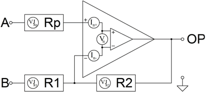
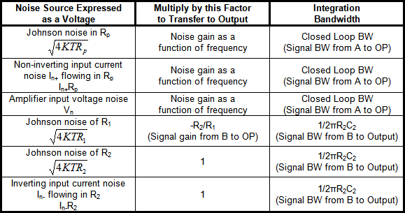
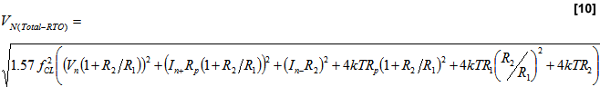
Figure 8 Engineers, who rarely appreciate quite such a rigorous analysis, define "maximum pk-pk noise" not as a value which is never exceeded, but one which is rarely exceeded. A pk-pk noise specification, therefore, must always be specified with a probability of its being exceeded. Analog Devices uses the widely-accepted convention that a good definition of "maximum pk-pk noise" is 6.6 times the RMS value, which is exceeded less than 0.1% of the time. Total Output Noise Calculations When working in the range of frequency where the op amp noise sources have a 1/f characteristic the calculations become more complex, but it is usually possible to choose an op amp with which this is not the case. If we consider the circuit in Fig 9, which is an amplifier consisting of an op amp and three resistors (Rp represents the source resistance at node A), we can find six separate noise sources: the Johnson noise (VJ) of the three resistors, the op amp voltage noise, and the current noise in each input of the op amp. Each has its own contribution to the noise at the amplifier output. (Noise is generally specified RTI, or referred to the input, but it is often simpler to calculate the noise at the output and then divide it by the signal gain (not the noise gain) of the amplifier to obtain the RTI noise).
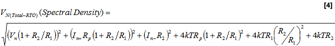
Figure 9 The RTO noise of the six noise sources is obtained by taking the square root of the sum of the squares of each separate noise term:–
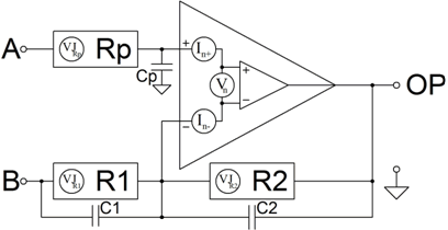
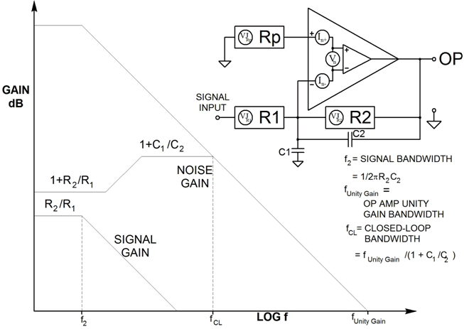
(Note that the Johnson noise (VJ) of a resistor is a square root (√4kTR)so the 4kTR terms are already squared.) If we compare the magnitude of each term (before squaring it) we can determine which noise sources are important. Any noise component which is less than 1/3 to 1/5 of the largest may usually be disregarded. The circuit in Fig 9 is a simplification. In real life there will be reactances, probably capacitive, in the system and its noise performance will vary with frequency. Fig 10 shows a second-order system, where capacitor C1 represents the source capacitance, stray capacitance on the inverting input, the input capacitance of the op amp, or any combination of these. C1 causes a breakpoint in the noise gain, and C2 is the capacitor which must be added to obtain stability. Capacitors C1 and C2 cause the noise gain to be a function of frequency, and the system peaks at high frequencies (assuming C2 is selected to give a critically damped second-order system).
Figure 10 A DC signal applied to input A (B being grounded) sees a gain of: 1 + R2/R1 = DC Noise Gain
At higher frequencies, the gain from input A to the output becomes: 1 + C1/C2 = AC Noise Gain
The closed-loop bandwidth fCL is the point at which the Noise Gain intersects the open-loop gain. A DC signal applied to B (A being grounded) sees a gain of: –R2/R1
with a high frequency cutoff determined by R2C2: Bandwidth (B to Output) = 1/2 These are the non-inverting and inverting gains and bandwidths, respectively, of the amplifier. The current noise of the non-inverting input, In+, flows in Rp and gives rise to a noise voltage of In+Rp, which is amplified by the DC noise gain [5], as are the op amp noise voltage, Vn, and the Johnson noise of Rp, which is If we consider these six noise contributions, we see that if Rp and R2 are low, then the effect of current noise and Johnson noise will be minimized, and the dominant noise will be the op amp's voltage noise. As we increase resistance, both Johnson noise and the voltage noise produced by noise currents will rise. If noise currents are low, then Johnson noise will take over from voltage noise as the dominant contributor. Johnson noise, however, rises with the square root of the resistance, while the current noise voltage rises linearly with resistance, so ultimately, as the resistance continues to rise, the voltage due to noise currents will become dominant. The noise contributions we have analyzed are not affected by which of the inputs A or B is used as the signal input, provided the other is connected to a low impedance ground (or some other fixed voltage reference), which is why the non-inverting gain (1 + R2/R1) which is seen by the voltage noise of the op amp, Vn, is known as the "noise gain" of the amplifier. Calculating the total output RMS noise of the op amp requires multiplying each of the six noise voltages by the appropriate gain and integrating over the appropriate frequency as shown in Fig 10. The root-sum-square of all the output contributions then represents the total RMS output noise. Fortunately, this cumbersome exercise may be greatly simplified in most cases by making some appropriate assumptions.
Figure 11 The noise gain for a typical second-order system is shown in Fig 12.
It is quite easy to perform the voltage noise integration in two steps,
but notice that because of peaking, the majority of the output noise due
to the input voltage noise will be determined by the high frequency
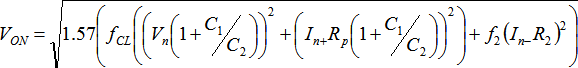
portion where the noise gain is 1 + C1/C2. This type of response is typical of second-order systems. The noise due to the inverting input current noise in R1 and R2 is only integrated over the bandwidth 1/2 Fig 12 also shows the amplifier noise sources in such a system. Disregarding resistor noise (which is not unreasonable at high frequencies since the higher currents used and the low impedance of capacitors at HF mostly require quite low values of resistor – resistor noise can almost always be ignored for resistors ≤1 kΩ, whose noise is approximately 4 nV/√Hz) the total noise of such a system is given by
The factor of 1.57 is the result of the 6dB/octave rolloff of single pole systems (see Fig 7).
Figure 12 In many high speed op amp systems further simplification is possible. Quite often the noise gain plot is optimized for fast settling time and is flat up to fCL, with at most one or two dB of gain peaking. All noise sources may therefore be integrated over the closed-loop op amp bandwidth using equation [4] which gives
It will probably be safe to neglect resistor noise here too, giving
Most high speed current feedback op amps have much greater current noise in the inverting input than in the non-inverting input. While it is probably a good idea to verify that this is the case for any particular amplifier the equation [11] can usually be simplified further with current feedback amplifiers to just
Noise Figures and Noise Factors
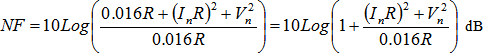
The concept is useful in RF, TV and other applications where 50Ω and 75Ω transmission lines and terminations are ubiquitous, but is useless for an op amp which may be used in a wide variety of electronic environments. Its principal use with op amps is its use by salesmen to confuse customers7, and it is very important to remember that it is meaningless to compare the noise figures of different devices unless the source resistances involved are identical. It is quite easy to calculate the NF of an op amp if we know its voltage (Vn) and current (In) noise densities and the source resistance (R) for which we wish to calculate the NF. For simplicity Vn and In should be expressed in nV/√Hz and nA/√Hz respectively. The noise spectral density of a resistance R at 290 K is
The spectral density of the current noise In flowing in R is simply InR, and of course the voltage noise density is Vn, so the total noise is
With many op amps, and especially for lower values of R, the InR term will be less than 30% of Vn and may often be disregarded, giving the simpler formula
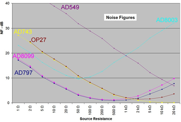
Figure 13 Fig 13 shows the variation of NF with source resistance for a number of Analog Devices op amps. Bipolar voltage feedback op amps have a minimum NF at source resistances of a few hundred ohms, above which the current noise takes effect, but FET op amps, with lower current noise, have very low NF at much higher resistances. The AD8003, which is a current feedback op amp with relatively high noise current (but excellent bandwidth and HF linearity) has a minimum NF around 50 Ω. No op amp can presently match the NF of purpose-built low noise RF amplifiers in 50 Ω systems, but their greater convenience of use may nevertheless be convenient in systems where the very lowest noise is not necessary. James Bryant 1 Johnson, John B. "Thermal Agitation of Electricity in Conductors" Physical Review 32.97, pp. 97-109, July 1928 and Nyquist, Harry "Thermal Agitation of Electric Charge in Conductors" Physical Review 32.110, pp. 110-113, July 1928. 2 http://en.wikipedia.org/wiki/Boltzmanns_constant 3 Shot, or Schottky (or as Walter Schottky himself called it, Schrot - literally "small shot"), noise is a statistical effect of charge carriers crossing a potential barrier such as a semiconductor junction. (Schottky, Walter "Regarding spontaneous current fluctuation in different electricity conductors" ANNALEN DER PHYSIK 57 (23): 541-567 December 1918 and "The calculation and review of the Schrot effect" ANNALEN DER PHYSIK 68 (10): 157-U10 July 1922) Resistors do not have shot noise (this is a simplification and not quite true but it is valid for most practical purposes). 4 The OP27 was introduced in 1980 at PMI, which later became a division of Analog Devices. It is still in widespread use after more than a quarter of a century. 5 Chopper stabilised op amps do not have 1/f voltage noise – the offset stabilisation process removes LF noise. However the same process makes the midband white noise relatively poor, so it is very unlikely that such devices would be chosen for a general purpose low noise amplifier, although if VLF noise is the only consideration they might be an excellent choice. 6 http://en.wikipedia.org/wiki/Gaussian_distribution 7 The salesmen are often pretty confused too. |