Digital Electronics Part III : Finite State Machines
These pages are © 2011-2015 Kael HANSON
A useful formalism for designing more complex digital circuits is
that of the finite state machine (FSM). Here, the circuit's function
is broken down into a collection of states and rules which determine when
the system moves from one state to another state. This concept can be
committed to paper by drawing what is called a state diagram. The state
diagram consists of nodes which represent the states and arrows (sometimes
called edges) which
give the possible transitions between states. The states usually are
named something which indicates the function of that state. It will be
seen that the state is held in flip flops, therefore there must be some
mapping made between the states and their representation in the FFs.
The arrows should be labeled with some condition which must be satisfied
in order for that state transition to take place. Typically the
 transitions are taken in response to external stimuli. Finally the state
machine must produce some desired configuration of outputs. State transitions
and the output configuration are mediated by combinational logic acting on
the inputs to the circuit and the circuit's internal state.
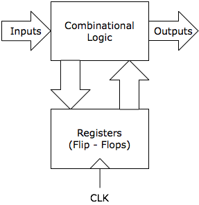
The basic design of the FSM is shown in the figure at right.
transitions are taken in response to external stimuli. Finally the state
machine must produce some desired configuration of outputs. State transitions
and the output configuration are mediated by combinational logic acting on
the inputs to the circuit and the circuit's internal state.
The basic design of the FSM is shown in the figure at right.
Here is the pattern for designing with the FSM formalism:
- Determine what states / transitions are needed in order to
solve the problem.
- Draw the state diagram, labelling the states and the edges.
- Develop a mapping between state and representation in FFs.
- Write out the state transition table (see below).
- Find the combinational logic which implements this state.
Finding the states and transitions
This is probably the most difficult part and requires some trial and
error. There is no magic formula to apply here. You must learn to
generalize by considering the examples given below.
State diagrams
Once you have the states and transition rules then drawing the diagram
is pretty easy. The states are usually drawn as circles with one or
more directed arrows giving paths to other states when certain criteria are met.
It's helpful to list all possibilities even if the state machine stays
in the same state (at the next clock edge) in which case you should draw
an arrow which loops back to the same state.
Mapping states to registers
In principle the designer is free to employ any mapping but in principle
there are two common general choices:
- Binary-coded states: in this case, the states are simply
numbered 1 through N and the flip-flops represent the number
in binary, thus, you need ceil(log2N) FFs to hold
the state. The order is still a free parameter here and very
often, well-chosen ordering can produce a simpler circuit,
- One-hot states: for the one-hot case, the designer
allocates 1 FF per state and when that state is active the
corresponding FF is logic HIGH and the rest are logic LOW.
This configuration is chosen as it usually produces simpler
combinational logic at the expense of exponentially more
flip-flops. One-hot mappings are often used in FPGAs where the
number of flip flops is very large.
State transition table
This is an extension of the truth table concept. The basic idea is to
list all flip flops in the FSM and any dependent inputs on the left side
of the table the flip flop configuration and the flip-flop bits representing
the next state and any
outputs on the right. Then, using the same techniques for implementation
of truth tables in combinational logic, derive the logic expressions for
each next-state FF bit and output signals.
Examples
It always helps to see a few examples of FSMs completely worked through.
Three examples of increasing complexity will be covered here.
Example #1: synchronous counter
We have already discussed the limitations of the ripple counter. A better
design for fast, robust counters uses an FSM and is called a synchronous
counter. The goal is this: make a circuit which counts on clock edges. For
clarity this example only is a 3-bit counter and doesn't include set or
reset inputs that would probably be found on a real synchronous counter.
States
The states are obvious in this example: there must be a distinct state for
every number in the counter. There is also a pretty obvious mapping of
state to flip-flop registers: the registers hold the binary-coded number.
Transitions
There are no external stimuli aside from a clock signal which only serves
to control the timing when the state transitions take place. The states
transition in the manner that state 0 goes to state 1 goes to state 2 ...
goes to state 15 goes to 0 ... and so on.
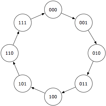
State diagram
The state diagram of this FSM is shown in the figure at left. The 3 bits
of the flip flops are shown inside the circles. Transitions are not labeled
as there is always and only one immediate exit from each state.
State transition table
| Q2 | Q1 | Q0 |
D2 | D1 | D0 |
|---|
| 0 | 0 | 0 | 0 | 0 | 1 |
| 0 | 0 | 1 | 0 | 1 | 0 |
| 0 | 1 | 0 | 0 | 1 | 1 |
| 0 | 1 | 1 | 1 | 0 | 0 |
| 1 | 0 | 0 | 1 | 0 | 1 |
| 1 | 0 | 1 | 1 | 1 | 0 |
| 1 | 1 | 0 | 1 | 1 | 1 |
| 1 | 1 | 1 | 0 | 0 | 0 |
The state transition table is simply written with the ouputs of the
current state of the flip flops (Qi) as inputs to the
combinational logic arrangement which must produce the next set of
inputs to the registers (Di on the right).
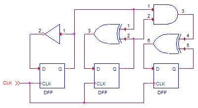
The logic expressions which implement this table are:
| D0 = Q0 |
| D1 = Q0⊕Q1 |
| D2 = Q2⊕(Q1
·Q0) |
Finally, the circuit implementation is given in the figure below:
Example #2: digital one-shot
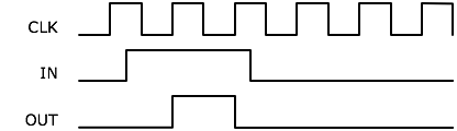
In the next example, we design a synchronous circuit which is the digital
equivalent of a monostable. This circuit takes a clock and an input
pulse. At the rising edge of the clock the output is brought high if and
only if the input is high and the output was not previously high. Another
way of looking at this is that the circuit creates output pulses synchronized
with the clock which are triggered by an input pulse but are only 1 clock
cycle in width, independent of the width of the input pulse. The circuit
cannot trigger again until it has detected a low on the input. Here is a
diagram which shows the response for an input two cycles wide:
States and transitions
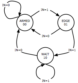 There are three possible states which can describe the life cycle of this
circuit:
There are three possible states which can describe the life cycle of this
circuit:
- ARMED
- The circuit is armed waiting for a trigger. IN=0 will keep the
circuit in ARMED state, IN=1 will cause it to go to EDGE.
- EDGE
- The circuit has just detected the leading edge on the input.
This state can only persist for one clock cycle. If IN=0 then the
FSM will go back to ARMED. If IN=1 then it must enter the
WAITING state, described next.
- WAITING
- The circuit saw the leading edge on the input but the input
is still high. That is to say that it is waiting, looking for the
trailing edge of the input pulse. As long as IN=1 the FSM will
remain here. As soon as IN=0 it can return to the ARMED state.
The state diagram for this FSM is shown at right:
State-to-register mapping
There are 3 states thus at least 2 flip flops are needed to hold the
state. I've chosen to enumerate the state ARMED = "00", EDGE = "01",
and WAITING = "10" to save a logic gate in making the output: the output
is high only for the EDGE state therefore it can be immediately identified
as the output of register 0 (recall that I write the bit strings
MSB first).
State transition table
| Q1 | Q0 | IN |
D1 | D0 | OUT |
|---|
| 0 | 0 | 0 | 0 | 0 | 0 |
| 0 | 0 | 1 | 0 | 1 | 0 |
| 0 | 1 | 0 | 0 | 0 | 1 |
| 0 | 1 | 1 | 1 | 0 | 1 |
| 1 | 0 | 0 | 0 | 0 | 0 |
| 1 | 0 | 1 | 1 | 0 | 0 |
| 1 | 1 | X | FORBIDDEN |
Now the state transition table involves an input and an output which
can be seen to be exactly equal to the register output, Q0.
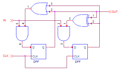
The expressions to realize this table are
| D0 = IN ·
Q0 ·
Q1
|
| D1 = IN ·
(Q0 ⊕ Q1) |
| OUT = Q0 |
And ... realized in discrete gates it looks like this:
Example #3: Cosmic Ray Muon Trigger
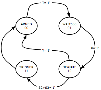 Once more we return to the muon trigger as we now have the capability
to finish the design all the way through the Michel electron capture
circuit. First, the states: 4 states are defined which described the
operational phases of the circuit at the highest level. This is a
multi-level design so, to tell you the truth, the WAIT500 and DLYGATE
states actually themselves activate sub-FSMs in the design (counters).
But, it helps to organize the design to separate these - a bit like
subroutines in a computer program. The 4 main states are:
Once more we return to the muon trigger as we now have the capability
to finish the design all the way through the Michel electron capture
circuit. First, the states: 4 states are defined which described the
operational phases of the circuit at the highest level. This is a
multi-level design so, to tell you the truth, the WAIT500 and DLYGATE
states actually themselves activate sub-FSMs in the design (counters).
But, it helps to organize the design to separate these - a bit like
subroutines in a computer program. The 4 main states are:
- ARMED
- The circuit is idling, waiting for a muon or something to
pass by. In this state, only the combination of S1 AND S2 AND
NOT S3 (S1 * S2 * S3'), here called 'T', becoming true will
cause the FSM to exit the state and enter WAIT500.
- WAIT500
- During this phase, the circuit will activate one of its
time sub-circuits to count out 500 ns in real time before
looking for the Michel electron. This 500 ns is a buffer
time to eliminate afterpulses or other noise in the PMTs
associated with the initial signal pulses. At the end of
500 ns the time sub-circuit asserts X which causes the FSM
to pass into the next state DLYGATE.
- DLYGATE
- In this phase, the circuit looks for a signal in either
S2 or S3 (U = S2+S3 below) for 15 us. If the 15 us period expires then the
circuit returns to the ARMED state (the other counter sub-circuit
asserts the Y signal). If either S2 or S3 are
asserted in the 15 us window then the FSM goes to TRIGGERED.
- TRIGGERED
- This is a one-clock-cycle state to raise a trigger pulse
for the data acquisition system. This state always exits
back to ARMED.
| STATE | Q0 | Q1 |
|---|
| ARMED | 0 | 0 |
| WAIT500 | 0 | 1 |
| DLYGATE | 1 | 0 |
| TRIG | 1 | 1 |
I didn't really pay much attention to the state enumeration. I chose
a binary encoding (2 FFs needed) and enumeration just based on the
time progression of the circuit. There could be better mappings and
since the state evolution logic is a bit complex here it may be better
to use the one-hot FSM encoding - in particulare since there are only
4 states. But, let's work through the binary method first. Encoding
is given in the table at right.
The state transition table is
given below:
| Q1 | Q0 |
T | X | Y | U |
D1 | D0 |
OUT (trigger) |
| 0 | 0 | 0 | X | X | X |
0 | 0 | 0 |
| 0 | 0 | 1 | X | X | X |
0 | 1 | 0 |
| 0 | 1 | X | 0 | X | X |
0 | 1 | 0 |
| 0 | 1 | X | 1 | X | X |
1 | 0 | 0 |
| 1 | 0 | X | X | 0 | 0 |
1 | 0 | 0 |
| 1 | 0 | X | X | 0 | 1 |
1 | 1 | 0 |
| 1 | 0 | X | X | 1 | 0 |
0 | 0 | 0 |
| 1 | 1 | X | X | X | X |
0 | 0 | 1 |
From this table, we can derive logic expressions for the state
transition logic:
|
D0 = Q0 ·
Q1 · T +
Q1 ·
Q0 · X +
Q0 ·
Q1 · Y · U
|
|
D1 = Q1 ·
Q0 · X +
Q0 ·
Q1 · Y
|
The full multi-page schematic
of this circuit is provided as a PDF.