Small but mighty, semiconducting qubits are a promising area of research on the road to a fully functional quantum computer. Less than one square micron, thousands of these qubits could fit into the space taken up by one of the current industry-leading superconducting qubit platforms, such as IBM’s or Google’s.
For a quantum computer on the order of tens or hundreds of qubits, that size difference is insignificant. But to get to the millions or billions of qubits needed to use these computers to model quantum physical processes or fold a protein in a matter of minutes, the tiny size of the semiconducting qubits could become a huge advantage.
Except, says Nathan Holman, who graduated from UW–Madison physics professor Mark Eriksson’s group with a PhD in 2020 and is now a scientist with HRL Laboratories, “All those qubits need to be wired up. But the qubits are so small, so how do we get the lines in there?”
In a new study published in NPJ Quantum Information on September 9, Holman and colleagues applied flip chip bonding to 3D integrate superconducting resonators with semiconducting qubits for the first time, freeing up space for the control wires in the process. They then showed that the new chip performs as well as non-integrated ones, meaning that they solved one problem without introducing another.
If quantum computers are to have any chance of outperforming their classical counterparts, their individual qubit units need to be scalable so that millions of qubits can work together. They also need an error correction scheme such as the surface code, which requires a 2D qubit grid and is the current best-proposed scheme.
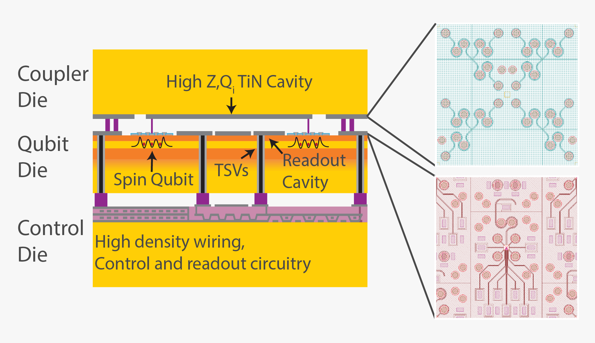
To attain any 2D tiled structure with current semiconducting devices, it quickly gets to the point where 100% of available surface area is covered by wires — and at that point, it is physically impossible to expand the device’s capacity by adding more qubits.
To try to alleviate the space issue, the researchers applied a 3D integration method developed by their colleagues at MIT. Essentially, the process takes two silicon dies, attaches pillars of the soft metal indium placed onto one, aligns the two dies, and then presses them together. The result is that the wires come in from the top instead of from the side.
“The 3D integration helps you get some of the wiring in in a denser way than you could with the traditional method,” Holman says. “This particular approach has never been done with semiconductor qubits, and I think the big reason why it hadn’t is that it’s just a huge fabrication challenge.”

In the second part of their study, the researchers needed to confirm that their new design was functional — and that it didn’t add disadvantages that would negate the spacing success.
The device itself has a cavity with a well-defined resonant frequency, which means that when they probe it with microwave photons at that frequency, the photons transmit through the cavity and are registered by a detector. The qubit itself is coupled to the cavity, which allows the researchers to determine if it is functioning or not: a functioning qubit changes the resonant frequency, and the number of photons detected goes down.
They probed their 3D integrated devices with the microwave photons, and when they expected their qubits to be working, they saw the expected signal. In other words, the new design did not negatively affect device performance.
“Even though there’s all this added complexity, the devices didn’t perform any worse than devices that are easier to make,” Holman says. “I think this work makes it conceivable to go to the next step with this technology, whereas before it was very tricky to imagine past a certain number of qubits.”
Holman emphasizes that this work does not solve all the design and functionality issues currently hampering the success of fully functional quantum computers.
“Even with all the resources and large industry teams working on this problem, it is non-trivial,” Holman says. “It’s exciting, but it’s a long-haul excitement. This work is one more piece of the puzzle.”
The article reports that this work was sponsored in part by the Army Research Office (ARO) under Grant Number W911NF-17-1-0274 (at UW–Madison) and by the Assistant Secretary of Defense for Research & Engineering under Air Force Contract No. FA8721-05-C-0002 (at MIT Lincoln Laboratory).