Peter Weix remembered for his technical, mentoring, and outreach efforts in physics

The Department of Physics mourns the loss of Peter Weix, who passed away January 13, 2023.

Peter began his career as an electronics technician in the U.S. Navy in 1984, where he serv­­ed until 1990. Following his Navy service, he worked as an electronics technician for several companies in California before joining the SLAC National Accelerator Laboratory at Stanford. At SLAC he was a Senior Technician with involvement on both the Stanford Synchrotron Radiation Lightsource and what is now the Linac Coherent Light Source. He also served as a Safety Officer with special emphasis on earthquake safety. Peter and his wife, Sheri, relocated to Wisconsin in 2001 so that Peter could join the Plasma Physics Group at UW–Madison where he worked for more than 20 years and advanced to Senior Instrumentation Specialist.

a man stands behind a lectern with physics gadgets behind him. he is wearing a costume that centers around the theme of time.
Peter Weix at the 2020 The Wonders of Physics annual shows | DEPARTMENT OF PHYSICS

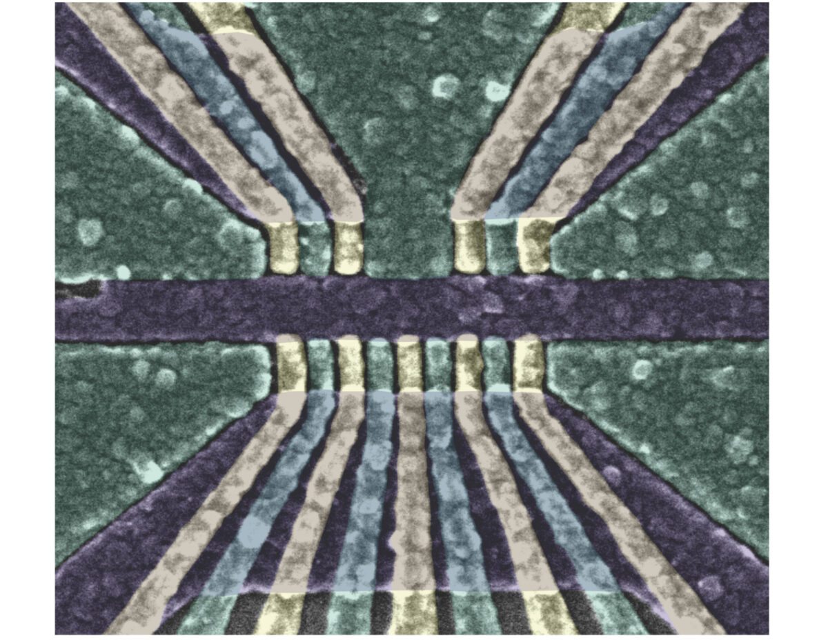
Peter’s work responsibilities at UW spanned a diverse range of technical operations for both the Madison Symmetric Torus (MST) and the Big Red Plasma Ball (BRB), two intermediate-scale experimental facilities for plasma physics research. He oversaw the mechanical and electrical aspects of the MST facility and its high-voltage pulsed-power systems, making sure the facility functioned as required, both technically and safely. He also oversaw all aspects of the high vacuum systems for both MST and BRB. There are many researchers, both in the local group and visiting collaborators, who relied on Peter’s efforts to make sure research projects stayed on track. Additionally, Peter directed key parts of large construction projects, such as the new programmable power supplies that replace MST’s passive capacitor-inductor circuits.

Peter’s involvement with plasma physics research included supervision of around 4-6 undergraduate students at any given time; he mentored an estimated more than 50 students during his time here. The students came from many areas of study, not just science and engineering, and rarely joined the group with the specific skills required to support research activities. Peter welcomed them into the department and provided them all with on-the-job training, teaching them skills and tricks of the trade to allow them to grow and become valuable members of the team.

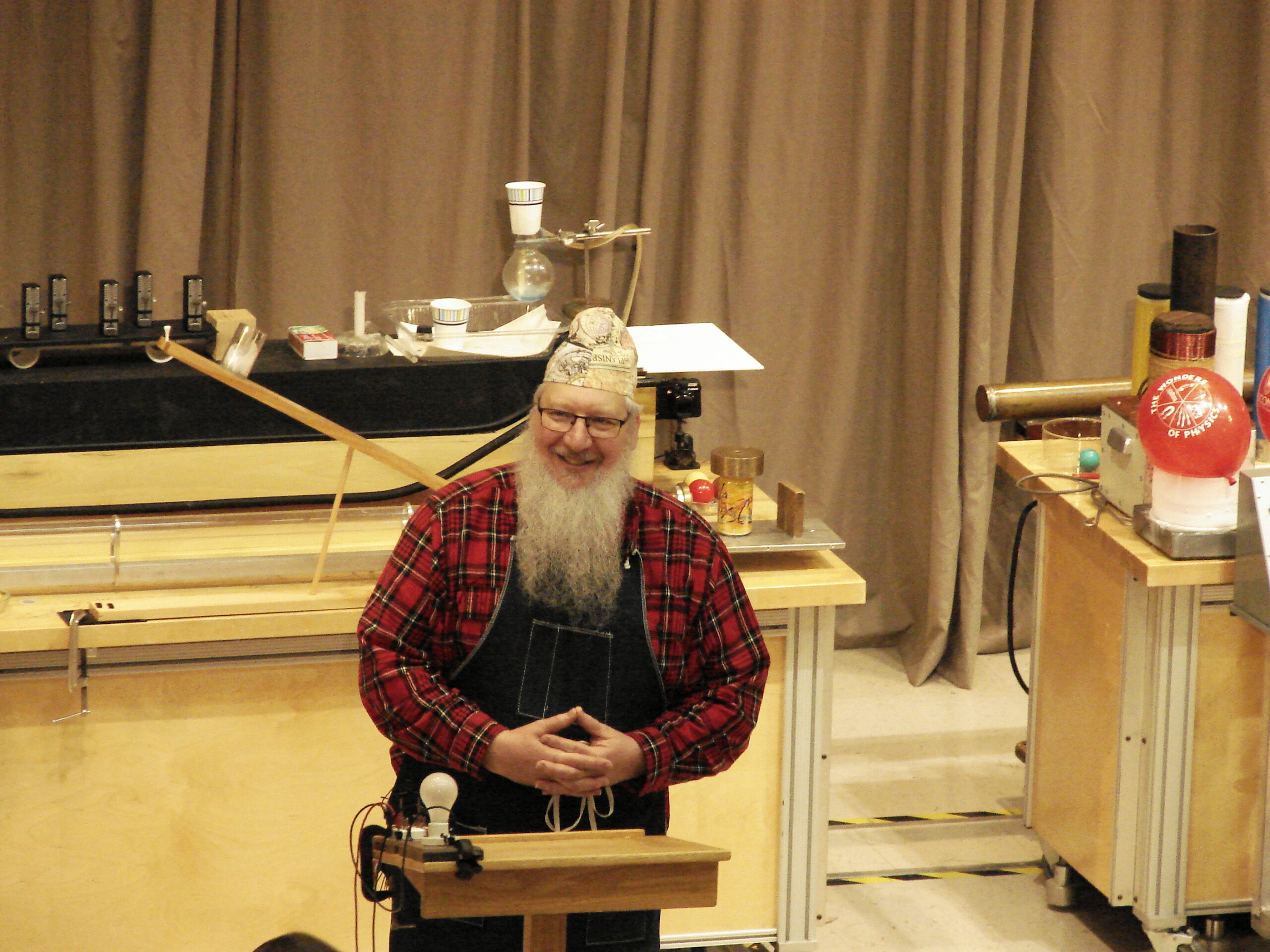
In addition to his dedicated service to the plasma group, Peter recognized the importance and value of physics outreach. He became a vital member of The Wonders of Physics program for over twenty years. His involvement started when one of the participants was suddenly unavailable at the start of one of the public shows. Peter saved the day by learning on the fly how to operate the complicated audiovisual system. His performance under pressure was impressive, and he was then asked to be the coordinator and main announcer for the approximately 200 shows that followed. Through the years, he provided ideas, elaborate props, personnel, wisdom, and a calming influence on the entire cast. He spent countless hours volunteering his time to the program.

In recognition of his many contributions to the department and university, Peter was awarded the 2022-23 George Ott award for staff excellence, the only department-level staff award given. He will be recognized at the annual Awards and Scholarship banquet in May.

Please visit the department’s tribute page to Peter Weix to submit and/or read stories from Peter’s colleagues.

Profs. John Sarff and Clint Sprott contributed to this piece

Finding some wiggle room in semiconductor quantum computers

a geometric pattern of lines in green, light gold, and black/dark purple, representing the qubit

Classical computers rarely make mistakes, thanks largely to the digital behavior of semiconductor transistors. They are either on or they’re off, corresponding to the ones and zeros of classical bits.

On the other hand, quantum bits, or qubits, can equal zero, one or an arbitrary mixture of the two, allowing quantum computers to solve certain calculations that exceed the capacity of any classical computer. One complication with qubits, however, is that they can occupy energy levels outside the computational one and zero. If those additional levels are too close to one or zero, errors are more likely to occur.

“In a classical computer, all the aspects of a transistor are super uniform,” says UW–Madison Distinguished Scientist Mark Friesen, an author on both papers. “Silicon qubits are in many ways like transistors, and we’ve gotten to the stage where we can control the qubit properties very well, except for one.”

That one property, known as the valley splitting, is the buffer between the computational one-zero energy levels and the additional energy levels, helping to reduce quantum computing errors.

In two papers published in Nature Communications in December, researchers from the University of Wisconsin–Madison, the University of New South Wales and TU-Delft showed that tweaking a qubit’s physical structure, known as a silicon quantum dot, creates sufficient valley splitting to reduce computing errors. The findings turn conventional wisdom on its head by showing that a less perfect silicon quantum dot can be beneficial.

Read the full story

Beating the diffraction limit in diamonds

by Daniel Heimsoth

Resolving very small objects that are close together is a frequent goal of scientists, making the microscope a crucial tool for research in many different fields from biology to materials science.

The resolution of even the best modern confocal microscopes — a common optical microscope popular in biology, medicine, and crystallography — is limited by an optical bound on how narrow a laser beam can be focused, known as the diffraction limit.

In a study recently published in the journal ACS Photonics, UW–Madison physics professor Shimon Kolkowitz and his group developed a method to image atomic-level defects in diamonds with super-resolution, reaching a spatial resolution fourteen times better than the diffraction limit achievable with their optics. And, because the technique uses a standard confocal microscope, this super-resolution should be available to any researchers that already have access to this common equipment.

profile photo of Aedan Gardill
Aedan Gardill

While methods to achieve super-resolution already exist, such as stimulated emission depletion microscopy (STED), nearly all of these methods either require the addition of special optics, which can be expensive and difficult to install, or specialized samples and extensive post processing of the data. The UW–Madison technique, which they call “super-resolution Airy disk microscopy” (SAM), avoids such barriers to entry.

“You can get this all for free with the existing setup that a lot of labs already have, and it performs almost just as well,” says Aedan Gardill, a graduate student in Kolkowitz’s group and lead author of the paper. “We were able to get resolution down to twenty nanometers, which is comparable with standard techniques using [STED].”

The ‘Airy disk’ in SAM refers to a key feature of light beams that gives rise to the diffraction limit but which the researchers turned to their advantage.

Confocal microscopes use laser beams of specific wavelengths to excite matter in a sample, causing that matter to emit light. On the microscopic scale, the laser beam does not create a solid circle of light on the sample in the same way a flashlight would.  Rather, light hits the object in a series of light and dark rings called an Airy pattern. Within the dark rings, the matter receives no light, which means it cannot be detected by the microscope’s light sensors.

The novelty of the SAM technique is in its two laser beam pulses, one spatially offset from the other such that the overlapping Airy patterns can distinguish between two closely spaced objects.

In their paper, the research team studied nitrogen-vacancy (NV) centers in diamond crystal, which are regions in the crystal lattice where one of two neighboring carbon atoms is replaced by a nitrogen atom, and the other is left empty. NV centers are known to have two different charge states based on how many electrons are in the defect, one that fluoresces and one that remains dark when yellow light is applied to them.

To resolve two NV centers separated by a distance less than the diffraction limit of the microscope, the SAM procedure first shines green light on them, preparing both centers into their fluorescent charge state. Then, a red laser is applied, offset such that only one of the two NV centers is in the dark ring of the Airy pattern and thus is not affected by the beam. The NV center that does see the red light is switched to the dark state.

a cartoon-rendered image of a microscope objective, with a red cylinder (light) hitting a sample that shows concentric rings of red and blue, as described in the text
Super-resolution Airy disk Microscopy uses the Airy disk (red pattern) generated by diffraction from an objective lens aperture (gray cylinder) to localize and control an emitter (here a nitrogen vacancy center in diamond) below the diffraction limit. Emitter fluorescence is suppressed everywhere except in a very narrow ring (blue donut).

“It goes to another dark charge state where it does not interact with yellow light,” Gardill explains. “But the initial bright charge state does interact with yellow light and will emit light.”

Finally, when the yellow laser is applied, one NV center emits light while the other does not, effectively differentiating between the two neighboring sites. By repeating these steps iteratively over a grid, the researchers could reconstruct a full image of the two nearby NVs with spectacular resolution.

The idea for this technique came as a bit of a surprise while the team was studying charge properties of NV centers in 2020.

“We tried the combinations of red-green, green-red, red-red, green-green with those first two [laser] pulses, and the one that was green then red, we ended up seeing this ring,” Gardill recounts. “And Shimon was like, ‘The width of the ring is smaller than the size of [the confocal image of] the NV. That is super-resolution.’”

This method could find wide use in many different fields, including biology and chemistry where NV centers are used as nanoscale sensors of magnetic and electric fields and of temperature in compounds and organic material. NV centers have also been studied as candidates for quantum repeaters in quantum networks, and the research team has considered the feasibility of using the SAM technique to aid in this application. Currently, the SAM method has only been applied to NV centers in diamond crystal, and more research is needed to extend its use to different systems.

That all of this can be done with hardware that many labs across the world already have access to cannot be overstated. Gardill reiterates, “If they have a basic confocal microscope and don’t want to buy another super-resolution microscope, they can utilize this technique.”

This work was supported by the U.S. Department of Energy, Office of Science, Basic Energy Sciences under Award #DE-SC0020313.

Daniel Heimsoth is a second-year PhD student in Physics. This was his first news story for the department.